
ASML Plans Larger High-NA EUV Chips for Nvidia-Scale AI Processors
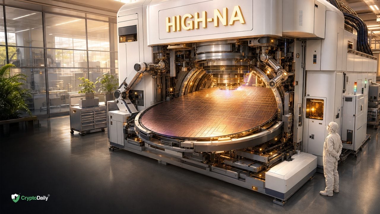
According to a September 7 report from Reuters, ASML plans to work with major chipmakers to adapt its High-NA EUV lithography tools for the large data-centre processors being designed by Nvidia and others.
High-NA EUV tools currently have a smaller mask exposure field than ASML’s established EUV machines.
AI systems require substantially more silicon. In an ASML presentation in January, the Dutch equipment maker said Nvidia’s 2024 Blackwell system requires 2.5 wafers, while a 2027 Rubin Ultra system requires 10 wafers.
High-NA EUV’s half-size exposure field
High-NA EUV is ASML’s next-generation extreme ultraviolet lithography platform. The company’s TWINSCAN EXE:5000 uses a 0.55 numerical aperture and is designed for 8-nanometre resolution.
The EXE:5000 has an exposure field half the size of conventional NXE systems, whose numerical aperture is 0.33. Its anamorphic optics enable finer resolution, but the smaller field creates a manufacturing challenge for very large AI dies.
ASML plans to work with major chipmakers on adapting High-NA EUV tools for large data-centre processors designed by Nvidia and other companies. Reuters described that effort as addressing the tools’ current smaller-mask limitation.
… Continue reading the full article at the original source below.